Analog Layout Design
Analog Layout Design Training
AGS QA Semiconductor approved training
Analog Layout Design Courses in Bangladesh
COURSE DESCRIPTION
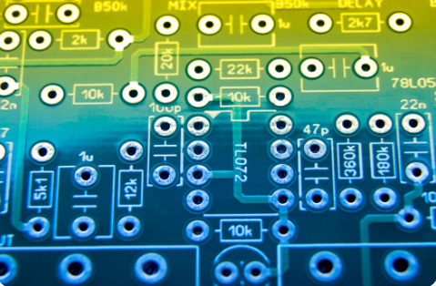
Analog Layout Design /Custom Layout Design /IC Layout Design course mainly focused on giving hands-on practical exposure in doing chip layout design for a given analog & mixed signal design. By end of the course you will learn to work in Linux environment, schematic entry in EDA tool, placement planning, analog and digital layout design, routing and physical verification checks like DRC, LVS for typical analog circuits such as Opamp, PLL, Bandgap, LDO and standard cells. You will also understand fixing deep sub-micron process issues like Antenna, Latchup, EM&IR.
IC Design Training Online/Chip Layout training/ Custom Layout Training
Eligibility:
Fresh Graduate in:
- Electronic & Electricals (E&E)
- Electronic Science and Technology
- Communication Engineering
- Microelectronics Science and Engineering
- Electronic or Computer or Information Science and Technology
- Other electronics-related disciplines
- Unemployed Engineering Graduate Individual below age of 30
Course Highlights:
- Deep understating of MOSFET device physics and various key analog circuit designs.
- Practical understanding of matching, shielding techniques.
- Hands on exposure in fixing layout violations such as DRC, LVS, Antenna, Latchup, EM&IR.
- Hands on experience in standard cell layout design, I/O Layout design, Memory Layout Design.
- Critical Industry standard project execution under the guidance of 12+ year’s industry expert.
- 24×7 Lab Support with classroom practice handouts and course material. Soft skills development,
- job oriented analog layout design training with 100% placement assistance.
Analog Layout Design training institute with placement
COURSE CURRICULUM
Module 1: Basics of Unix/Linux
- 1 - Introduction and Working knowledge of UNIX/LINUX commands
- 2 - File handling skills in UNIX/LINUX
- 3 - Introduction to programming languages used in IC-Design
Module 2: Introduction to Electronics and Circuits
- 4 - Revision of Analog, Digital electronics, RLC Circuits
- 5 - Introduction to MOSFET Theory & CMOS Circuits
Module 3: Design for Manufacturability Checks
- 6 - Latch-up, Antenna Effect
- 7 - Electro-migration (EM), IR Drop & Self-Heat (SH)
- 8 - Electrical rule check (ERC) and Design rule check (DRC)
Module 4: Deep sub-micron process challenges
- 9 - Well proximity Effect (WPE), Length of Diffusion (LOD)
- 10 - Shallow trench Isolation (STI)
- 11 - Metal Density effects
Module 5: Introduction to IC Circuit Layout
- 12 - CMOS Fabrication Technology
- 13 - Introduction to Second order effects in MOSFET
- 14 - CMOS Stick Diagrams
- 15 - Introduction to IC Circuit Layout and Physical Verification tools
- 16 - DRC, LVS, ERC and Antenna checks
Module 6: Analog Circuit Simulations
- 17 - Introduction to Analog Design Environment
- 18 - Design of Inverter circuit
- 19 - Design and Parasitic Extractions of Inverter Layout
- 20 - Analysis of the INV Characteristics
- 21 - Understanding of the time delay concepts
Module 7: Analog Circuit Layout Design Techniques
- 22 - Common centroid & Interdigitation matching techniques
- 23 - Critical signals shielding techniques
- 24 - Constraint & Module based floor planning techniques
- 25 - Guard / Seal ring techniques
Module 8: Custom Layout Techniques
- 26 - STD Cell Layout design techniques
- 27 - I/O Layout design techniques
- 28 - Memory Layout Design techniques
Module 9: Basic Analog Circuit Layout Design
- 29 - Layout Design & Physical Verification of Operation amplifier
- 30 - Layout Design & Physical Verification of Voltage Controlled Oscillator
- 31 - Layout Design & Physical Verification of Band gap Circuit
- 32 - Layout Design & Physical Verification of Current mirror
Module 10: Layout Design of Critical Analog Circuits
- 33 - Advanced/Critical Analog Circuits
- 34 - Complete Physical Verification Checks required for a Successful tape-out
Module 11: Industry standard Project Execution
- 35 - Working on Critical Analog Circuits that are important in Industry Module
Module 12: Mock Interviews & Personality improvement
Analog Layout Design /Custom Layout Design /IC Layout Design course mainly focused on giving hands-on practical exposure in doing chip layout design for a given analog & mixed signal design. By end of the course you will learn to work in Linux environment, schematic entry in EDA tool, placement planning, analog and digital layout design, routing and physical verification checks like DRC, LVS for typical analog circuits such as Opamp, PLL, Bandgap, LDO and standard cells. You will also understand fixing deep sub-micron process issues like Antenna, Latchup, EM&IR.
20 Students
Duration: 5 Months
Register Now
Social Network
Get in Touch section
Let’s discuss your next AGS QA Semiconductor design & training.
Have an idea in mind? We’re here to listen and provide the right guidance. Get in touch to discuss how we can turn your vision into reality. Our team experts to support you through every step of your project journey.